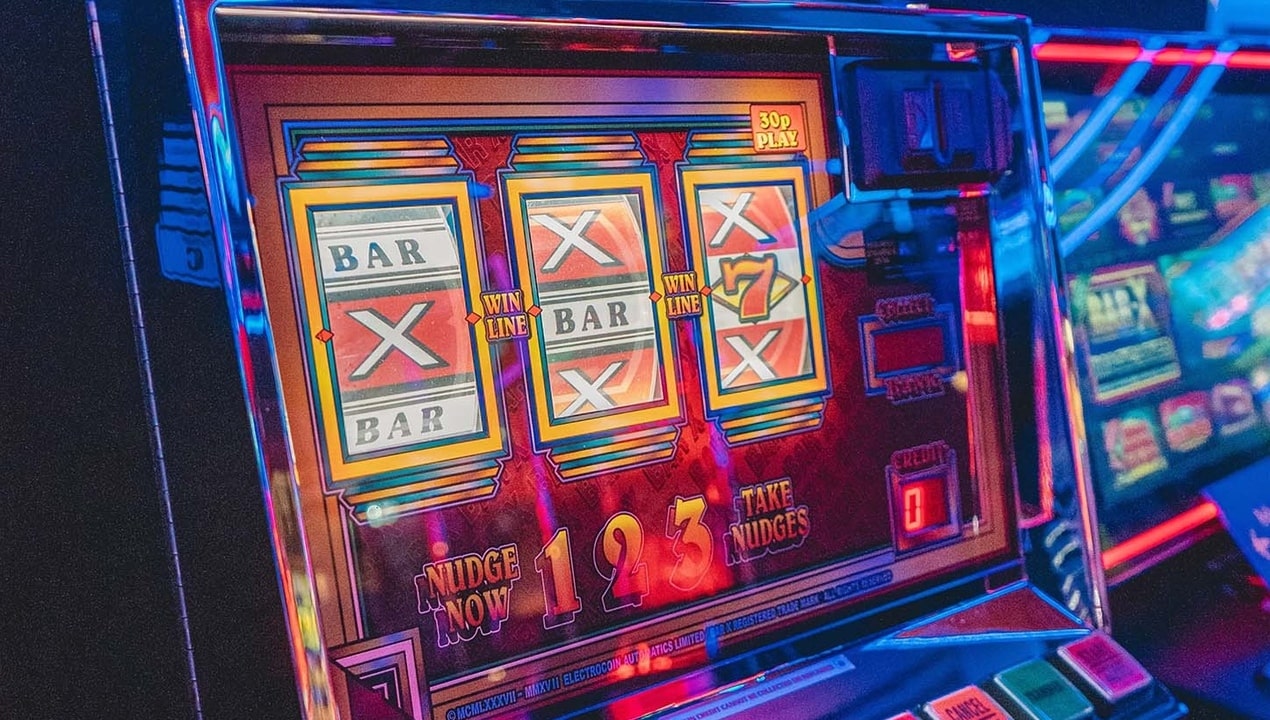
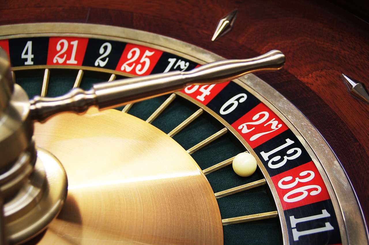
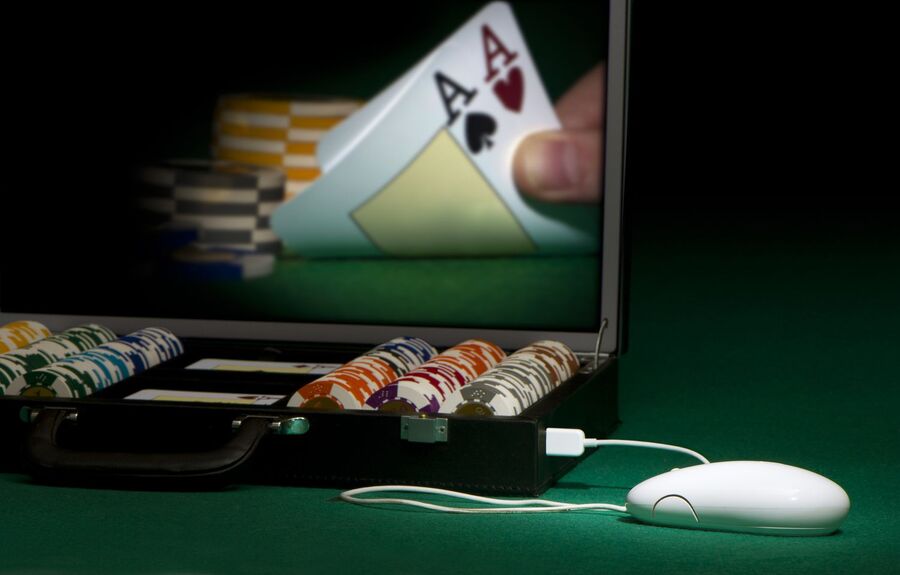
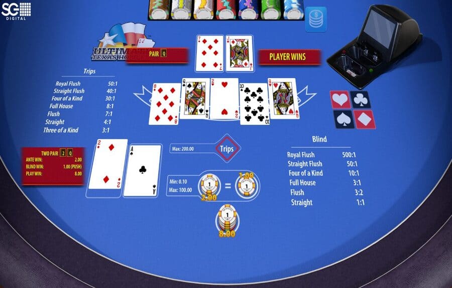
Silicate Crystal Structures
We are integrating ultra low light, active night vision and 3D point cloud into a single sensor. These cameras will have major benefits over current generations with minor added cost. We are a Singapore-primarily based business established to provide globe-class compelling and cost-effective solutions to improve connectivity and quality of life for every person. Xceler Systems is building a new kind of processor and platform to allow the next generation Intelligent Edge. The brain-like graph engine is built using “Digital Neurons,” with the capability to dynamically type thousands of synapses each clock cycle for computing.
Previously, it has also been shown from the very first principle based atomistic simulations that Si-wealthy SiC nano-clusters can be very stable and can have tunable power gaps . In the bulk limit, the non-stoichiometric SiC may perhaps offer such possibilities as well, so we have studied Si-rich SiC with periodic boundary circumstances in this function. The atoms in the crystal structure of the silicon lattice is arranged in a ‘diamond cubic’ formation. In this orientation, each and every silicon atoms has four neighbouring silicon atoms with which it is bonded with. The lattice constant—the distance among atoms in the atomic unit cell—is 5.431 Å, and the atomic density of the material is five.02×1022 atoms/cm3. Silicon in a cubic diamond structure currently plays a significant part in the photovoltaic business.
Once more, the bonding amongst the atoms goes on and on in 3 dimensions. For clean Si surfaces, a specifically steady reconstruction is the Si7×7, with a diamond-shaped unit cell 7 atomic spacings on every side. The formation enthalpies per atom for diamond, FeSi, wurtzite and 6H structures with silicon substitution for carbon web-sites. Silicon-rich silicon carbide of diamond, and 6H structures in their 2 × 2 × 2 supercell representation.
Because of the value of the material for electronics, it is vital to generate a huge single crystal. The electronics industry has invested heavily in the improvement of significant single crystals of silicon to make advanced electronic equipment. The solar cells are then manufactured and aligned on the wafers. Subsequent, two layers of material are laid over the top rated of the wafers to protect and preserve the wafer structures. On one particular side of these layers are deposited a thin layer of monolithic material referred to as the deposited oxide layer. This layer is extremely effective at reflecting and removing any excess power that would otherwise pass by way of the thin layers of crystalline material that kind the base of the wafer.
CoolKit ZB-GW04 USB dongle (a.k.a. easyiot stick)USB connected adapter (CoolKit ZB-GW04 USB dongle, also known as “easyiot stick”) widly accessible on the a knockout post web from China. Elelabs ELU013 and Popp ZB-STICKUSB connected adapters (Elelabs ELU013 and Popp ZB-STICK ). ITead Sonoff Zigbee 3. USB Dongle Plus V2 model “ZBDongle-E”USB connected adapter with external antenna.
Produced utilizing semiconductor lithography strategies, the capacitors are intended for higher-end applications such as in-package energy supply decoupling for mobiles and high-efficiency computing. The group was in a position to activate the neurons utilizing pulses of light to heat up the silicon particles, causing current to flow by way of the cells. The quantity of protons in the nucleus of an atom is named atomic number.
Silicone adhesives provide the capability to bond ceramic material with dissimilar substrates that have chemical compositions that are unsuitable for bonding with ceramics. A major advantage of silicone adhesives is how lengthy they are able to sustain their bond regardless of the environment. This single feature makes them an excellent supply for several applications including medical ones.
Blue for silicon, smaller brown for carbon and red for added silicon doped for carbon sites. This is a silicon (a.k.a. diamond) lattice based off the image in Shockley. The orange, green, and purple planes represent the planes with Miller indices , , and , respectively. Floating zone is a crucible absolutely free technique applied to produce monocrystalline Si by melting and solidify polycrystalline Si in the type of ingot. It is usually used in the production of high resistivity monocrystalline Si which needs minimum oxygen level and other impurities for the finest performance. Other procedures accessible to make monocrystalline Si are Czochralski and directional solidification strategy.
If you do function at a place like this, it’s very important that you put on an suitable dust mask or respirator. Given that the components in silicone adhesives are taken from natural components, it has incredibly little impact on the atmosphere. Silicone adhesives are resistant to most chemical compounds and are non-chemical reactive, a issue full article that emphasizes its environmental security. Although silicone adhesive forms a pretty safe and tight bond, it does not harden and come to be rigid. For a lot of applications, flexibility in a bonding agent is a important necessity due to the fact most materials flex with environmental modifications.
To answer these questions, let’s figure out some terminologies relate to silicone initially. Silicone and rubber are each elastomers, however, even though they share some characteristics, they do have several differing properties. Dr. Helmenstine holds a Ph.D. in biomedical sciences and is a science writer, educator, and consultant.
Because silicon is so abundant and quickly worked with, it is not tough to make issues with it. In contrast to other materials, silicon is affordable and abundant in nature. Because silicon is a reasonably uncomplicated substance, scientists can develop crystals of the material, which are equivalent to diamond. Silicon is the second-most abundant element on earth, and it can be found pretty much anywhere on Earth. If you are curious about what these supplies look like, check out these photographs. Exotic forms of silicon have been discovered that can be utilised in explosives.
Silicon is the most abundant metalloid element in the Earth’s crust. The element has a metallic luster, but it is also brittle and a poor conductor of electrical you could look here energy. Silicon is typically tetravalent, while it can also be bivalent.
Its low-toxicity and lengthy shelf life make it a suitable material for use in explosives. The carbonates of silicon are amorphous, high-frequency compounds formed when silicalite is subjected to stress. They contain 1 framework silicon atom and two helium nuclei. The unidentate carbonates are most stable, but also have some higher-frequency elements. Throughout the supernova stage, silicon combines with helium nuclei to make other components.
The similarity in structure of quartz and diamond explains its hardness, and quartz is also transparent/translucent, which gives it a use in jewellery. If you would like a quotation or additional information and facts about our products, please leave us a message, will reply you as quickly as possible. The measurement of Si crystal diameter and allowable deviation shall be carried out in accordance with the provisions of GB/T 14140.
RECENT COMMENTS